Orientation Mapping
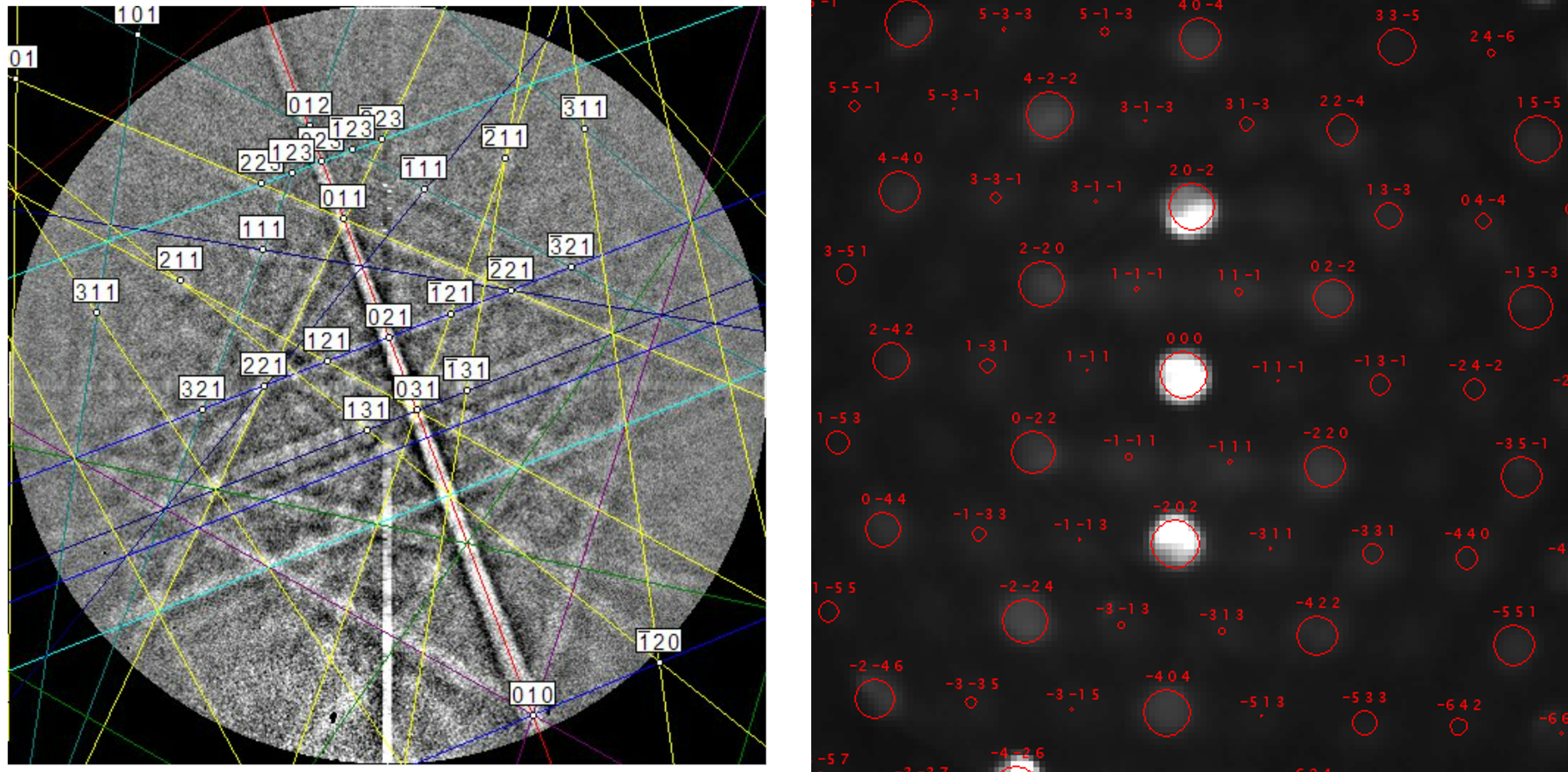
Analyzing a material's grain structure is pivotal for understanding properties like strength, electronic and ionic conductivity, and more. In the electron microscope, there are two main approaches for investigating grain structure via orientation mapping of the individual grains in a material: indexing Kikuchi diffraction patterns or indexing diffraction spots from an electron diffraction pattern.

Choosing the best diffraction indexing approach depends on the sample thickness and the desired analysis. For example, Kikuchi pattern indexing is utilized in electron backscatter diffraction (EBSD) analysis in a scanning electron microscope (SEM), where a bulk sample is used, and a large area (several microns in size or greater) must be analyzed. Higher resolution analysis (~1 nm resolution or smaller) requires using a transmission electron microscope (TEM), where the sample must be thin enough to be electron transparent, making the individual spot indexing approach more appropriate.
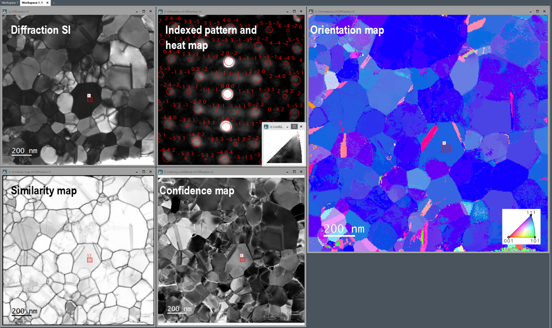
An orientation map in the TEM can be generated by acquiring a 4D STEM dataset and indexing the diffraction spot pattern at each pixel position. Gatan cameras with the STEMx® package can rapidly acquire high-quality 4D STEM data. From there, the STEMx OIM features in DigitalMicrograph use an automated template-matching approach to index patterns and generate orientation maps. The only other information required is the material structure (in a CIF file format) for STEMx OIM to simulate and index diffraction patterns. Orientation map data generated by STEMx OIM can be imported into EDAX OIM Analysis for further processing or linked with EELS, EDS, and other 4D STEM analysis data thanks to eaSI™ technology in DigitalMicrograph.
