WHAT IS Cathodoluminescence?
After being excited by an electron beam, many materials emit light in a captivating display known as cathodoluminescence (CL). This light spans the spectrum from ultraviolet to visible and even infrared wavelengths, showcasing the hidden wonders within the material. However, the reach of a CL system is defined by its carefully chosen internal optics and detectors. By exploring the specific wavelengths emitted through spectroscopy, we gain a deeper understanding of the material's essence. Additionally, delving into the nuances of the collected light, including analysis of polarization and emission angles, unveils even greater insights into its fascinating characteristics.
The electron beam of an electron microscope can be focused to a diameter of just a few nanometers or less, forming a highly focused energetic probe capable of exciting metals, semiconductors, and insulating samples. This finely focused electron beam can be scanned across a specimen, producing CL images or maps with remarkable spatial resolution, exceeding that of optical spectroscopies by over tenfold. By adjusting the microscope's acceleration voltage to influence the electron beam's interaction volume with the electron's landing energy, we can delve into the varying depths of a specimen to explore its evolving characteristics.
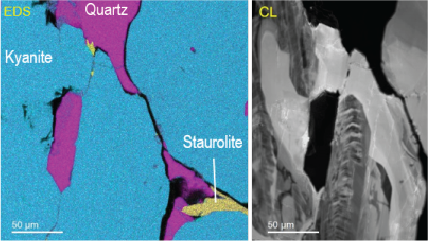
CL can harmoniously be combined with other electron microscopy techniques, such as electron energy loss spectroscopy (EELS), electron backscatter diffraction (EBSD), or energy dispersive spectroscopy (EDS), creating a powerful synergy. This integration positions CL as a compelling technique for diverse applications and groundbreaking research, particularly in semiconductors, plasmonics, and geology. By analyzing the emitted light, we unveil crucial insights into a material’s structural and functional properties, offering revelations that transcend the limitations of other methods.

As described above, many different types of CL experiments can be conducted. The table below outlines some experiment types and their potential applications.
| Modalities | Example applications |
|---|---|
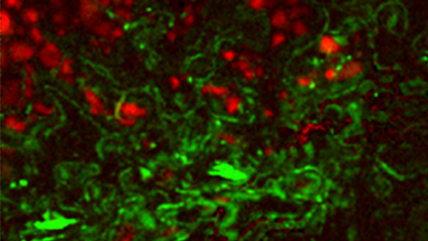
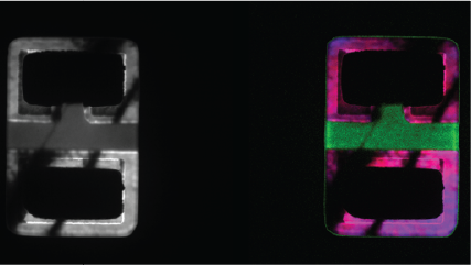
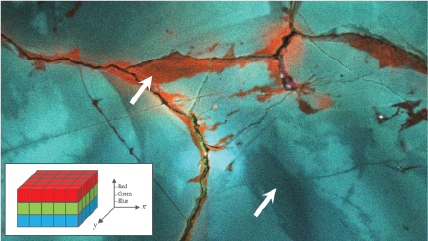
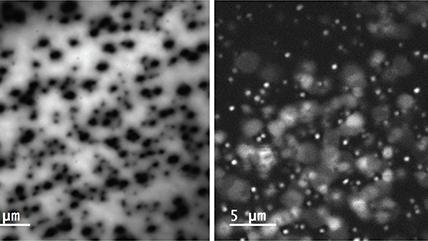
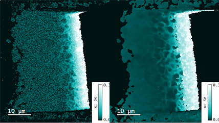
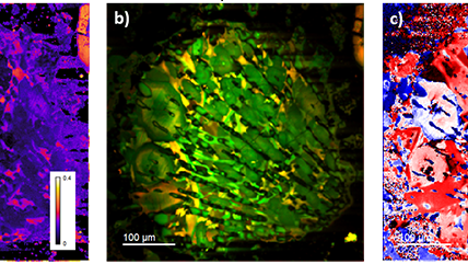
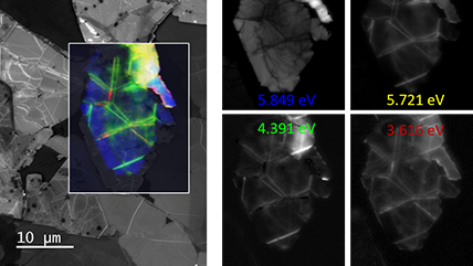
| Unfiltered Imaging / Filtered Imaging | Creates a map that showcases the dynamic variations in CL intensity, where the emitted light is filtered to unveil information at selected wavelengths. This technique illuminates the intricate textures in mineralogy, zonation, overgrowths, and micro-cracks, revealing extended defects in semiconductor materials and devices. |
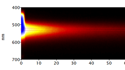
| Spectroscopy | Captures a CL spectrum that unveils the intensity variation by wavelength. This can reveal radiative impurities such as trace elements, perform composition metrology in compound semiconductors, and investigate exciton luminescence signals. |
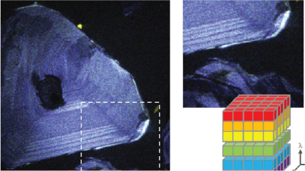
| Spectrum Imaging (SI) | Collects a CL spectrum at each point of a map, revealing the qualitative (normally) composition or strain mapping of an alloy. |
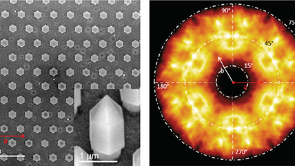
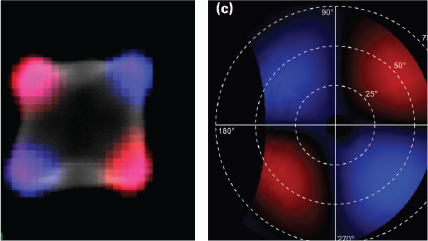
| Angle-resolved CL (ARCL) | Determines the emission pattern of nanostructures and light-emitting devices. |
| Wavelength and angle-resolved CL (WARCL) | Uncovers photonic band structures and energy-momentum spectroscopy. |
| Polarization resolved | Retrieves the full polarization state of the emitted light. |
For more information on CL please visit www.WhatisCL.info, an educational site.


Live color cathodoluminescence imaging for your scanning electron microscope.

DigitalMicrograph, also known as Gatan Microscopy Suite, drives your digital cameras and surrounding components to support key applications including tomography, in-situ, spectrum and diffraction imaging, plus more.

Digital beam control and image processing to enhance the photographic quality of your digital images.


Enabling optically-coupled transmission electron microscopy to reveal nanoscale structural, optical, and electronic properties

Enabling optically-coupled transmission electron microscopy to reveal nanoscale structural, optical, and electronic properties


Applications
|
|
|
|
Monarc detector

Cathodoluminescence in the TEM
|
|
|
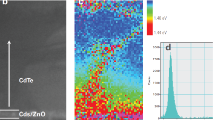
Mapping the electronic bandgap of semiconductor compounds with milli-electron volt accuracy |
|
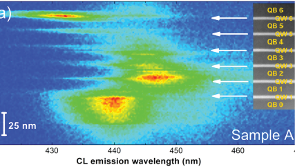
Nano-cathodoluminescence enables the design of light-emitting diodes with higher efficiencies |