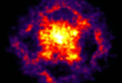
4D STEM is the capture of a full 2D diffraction pattern at each pixel position in a STEM map.
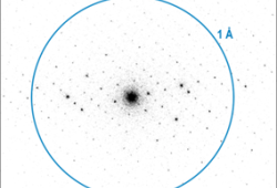
Capturing electron diffraction patterns from small crystals while the specimen is continuously rotated in the TEM
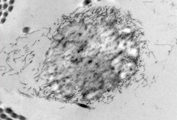
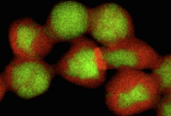
Award winning, high resolution imaging tools help you to understand ultrastructure of biological and inorganic specimens.
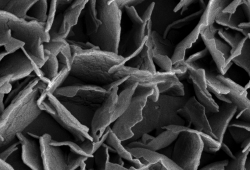
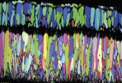
Electron backscatter diffraction (EBSD) provides crystallographic orientation and phase information necessary to understand materials' microstructure-property relationships.
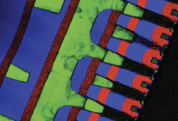
Electron energy loss spectroscopy (EELS) and energy-filtered transmission electron microscopy (EFTEM) for materials analysis.
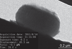
Real-time observation of growth processes, chemical reactions and oxidation, irradiation effects, mechanical, magnetic, and ferroelectric properties.
Unique insight into the chemical and electronic properties of materials at the microscopic level.
