什么是阴极荧光?
在电子束的激发下,许多材料会发出迷人的光,也就是阴极荧光 (CL)。它的发光波长范围覆盖了从紫外到可见光甚至红外波长,能够展示材料中隐藏的奇妙之处。但是,CL 系统的表征范围由精心挑选的内部光学元件和探测器决定。通过谱学研究发射出的特定波长,我们可以更深入地了解材料的本质。更进一步,深入研究收集到的光的细节,包括对偏振和发光角度的分析,可以揭示令人着迷的发光特性更深层的洞见。
电子显微镜的电子束可以聚焦到几纳米或更小的直径,形成一种高度聚焦的能量探针,能够激发金属、半导体和绝缘样品。这种高度聚焦的电子束可以在样品上进行扫描,生成高空间分辨率的 CL 图像或分布图,比光学光谱学的分辨率高出十倍以上。通过调整显微镜的加速电压来影响电子束与电子着陆能量的相互作用体积,我们可以深入探究样品的不同深度,以探索其不断变化的特性。
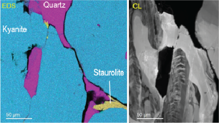
CL可以与其它电子显微镜技术,例如如电子能量损失谱 (EELS)、电子背散射衍射 (EBSD) 或能量色散谱 (EDS) 和谐地结合在一起,创造出强大的协同效应。这种结合使CL成为具有吸引力的技术,可用于各种应用和开创性的研究,特别是在半导体、等离子体光学和地质学领域。通过分析发射出的光,我们可以揭示出材料的结构和功能特性的重要信息,这些信息超越了其他方法的局限性。

如上所述,能够实施许多不同种类的 CL 实验。下面的表格简要描述了若干实验种类和它们潜在的应用。
| 表征模态 | 示例应用 |
|---|---|
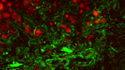
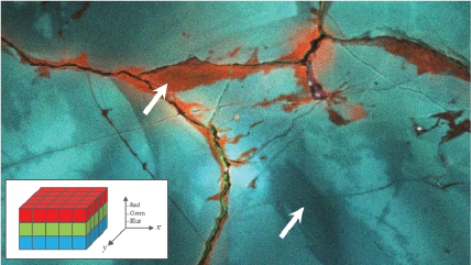
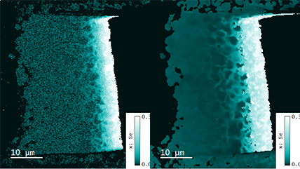
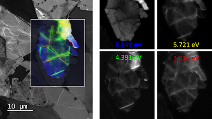
| 无过滤成像/过滤成像 | 构成分布图,展示出 CL 强度的动态变化,对发光进行过滤后来揭示特定波长上的信息。这一技术展现了成矿的复杂纹理,成带,过度发育和微裂纹,揭示半导体材料和器件中的扩展缺陷。 |
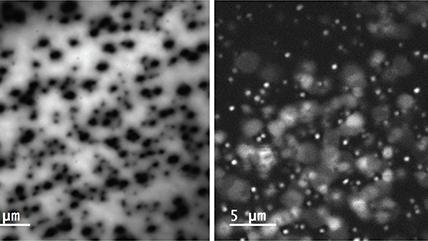
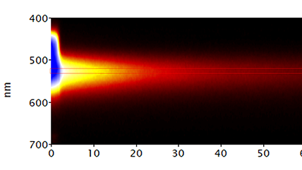
| 谱学 | 采集的 CL 光谱体现了不同波长上的强度变化。能够揭示诸如痕量元素这种的发光杂质,或对化合物半导体进行成分量测,以及研究激子发光信号。 |
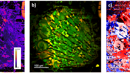
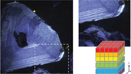
| 谱成像 (SI) | 在一个分布图中的每个点都采集一条 CL 光谱,从而揭示合金中 (通常) 定性的成分或应变分布。 |
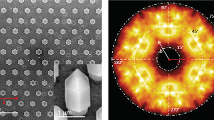
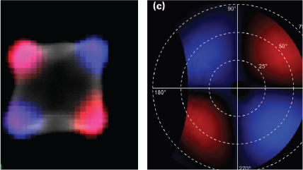
| 角度分辨 CL (ARCL) | 确定纳米结构和发光器件的发光花样。 |
| 波长-角度分辨 CL (WARCL) | 揭开光学支能带结构以及能量-动量谱学。 |
| 偏振分辨 | 从发光中提取所有的偏振态。 |
如遇了解更多 CL 相关的信息,请访问www.WhatisCL.info, 我们的教育网站。


DigitalMicrograph,或称为 Gatan Microscopy Suite,驱动您的电子相机和其他附件以支持一系列重要应用,包括断层扫描、原位、谱学和衍射成像等。


Enabling optically-coupled transmission electron microscopy to reveal nanoscale structural, optical, and electronic properties

Enabling optically-coupled transmission electron microscopy to reveal nanoscale structural, optical, and electronic properties

 —— Gatan Monarc 阴极荧光(CL)探测器")


应用
|
|
|
|
Monarc 探测器

Cathodoluminescence in the TEM
|
|
|
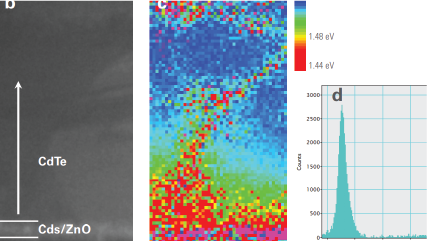
Mapping the electronic bandgap of semiconductor compounds with milli-electron volt accuracy |
|
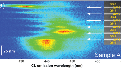
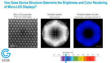
Nano-cathodoluminescence enables the design of light-emitting diodes with higher efficiencies |