Paolo Longo, Ph.D., Gatan, Inc.
Sample courtesy of University of Glasgow
Microscope courtesy of Professor Ray Carpente at Arizona State University, Tempe, AZ
Acknowledgement to Dr. Toshiro Aoki at Jeol USA (now at ASU) for helping set up microscope for experiment.
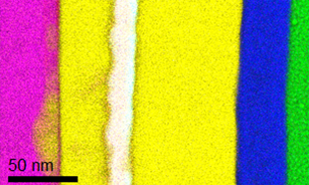
Fast DualEELS color map of a AuGeNi metal alloy ohmic contact for the fabrication of III-V transistor device structures; absolute compositional analysis also carried out
AuGeNi ohmic contacts are widely used as they show a low contact resistivity and are typically compatible with the fabrication of III-V MOSFET devices1. However, they have the drawback of poor uniformity due to diffusion of the Au into the III-V substrate. This diffusion is dependent on temperature used during the annealing process after deposition of Au, Ge and Ni. It is clear that the performance of this type of contact will be influenced by both the material present and degree of roughness at the interface with the III-V substrate.
Methods
Probe-corrected Jeol ARM 200 TEM/STEM microscope; S-FEG emission gun; Enfinium™ ER system; voltage: 200 kV; STEM mode; EELS low-loss spectrum (200 – 2200 eV): 0.006 ms; EELS core-loss spectrum (700 – 2700 eV): 0.99 ms; dataset size: 512 x 307 pixels; total exposure time: 6 min
