Data courtesy of Dr. U. Jahn, Paul-Drude-Institut für Festkörperelektronik.
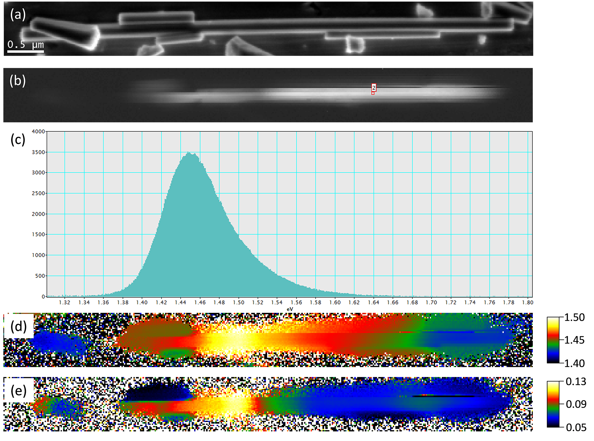
Cathodoluminescence spectrum-imaging of a gallium arsenide (GaAs) nanowire
(a) Secondary electron image of a 200 nm diameter GaAs nanowire; (b) Cathodoluminescence spectrum-image displaying energy plane 1.46 ± 0.02 eV; (c) Individual cathodoluminescence spectrum extracted from spectrum-image with single peak at 1.45 eV; (d) Map of central energy of luminescence; change in wavelength is associated with a transition from zincblende (1.425 eV) to wurtzite crystal structure; wurtzite phase is calculated to have 55 meV larger band gap than zincblende phase; (e) Map of FWHM along nanowire. FWHM remains constant for zincblende portion of nanowire but varies considerably in wurtzite phase.
Spectrum-image contains 400 x 41 pixels and was acquired at a rate of 10 ms/pixel (total acquisition time 3 min) in FE-SEM at room temperature. Images (a) and (b) acquired simultaneously; images (d) and (e) were calculated using NLLS routine of Gatan Microscopy Suite® software.

