Data courtesy V. B. Ozdol et al., National Center for Electron Microscopy, Lawrence Berkeley National Laboratory and Department of Materials Science and Engineering, University of California, Berkeley, California.
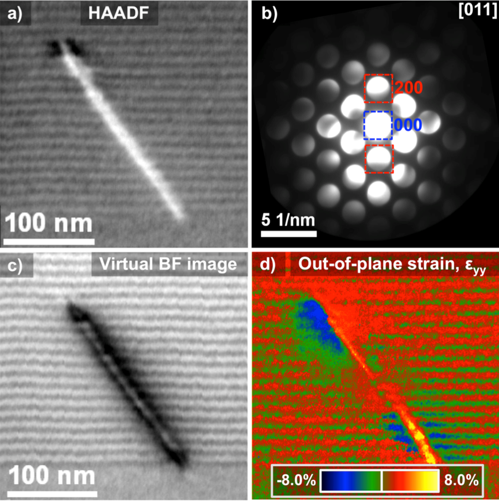
Nano-beam electron diffraction full 2D strain mapping
a) HAADF image of a GaAs/GaAsP multilayer laminate; b) Integrated diffraction pattern of the superlattice structure along the [011] zone axis; c) Virtual BF image extracted from 4D data cube quantifying strain down to 1.2 nm resolution in full 2D area in eyy; d) exx strain for same area shown.

