Paolo Longo, Ph.D., Gatan, Inc.
Sample courtesy of Dr. Pavel Potapov at Global Foundries, Dresden, Germany
Microscope courtesy of Dr. P. Rice and Dr. T. Topuria at IBM (Almaden), San Jose, CA
Acknowledgements to Dr. P. Rice and Dr. T. Topuria at IBM (Almaden), San Jose, CA for helping set up microscope for experiment.
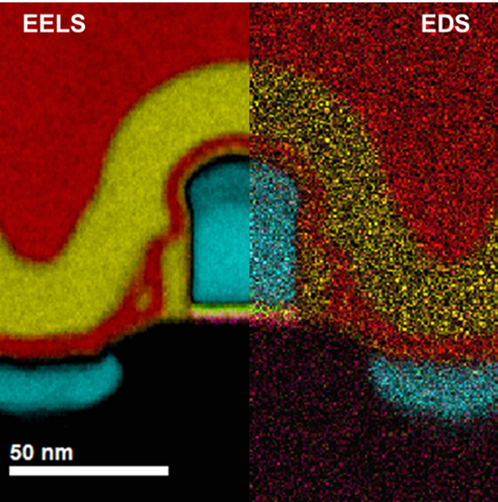
32 nm Transistor device
Methods
probe-corrected Jeol ARM 200 TEM/STEM microscope
C-FEG emission gun
GIF Quantum® ER system
Jeol Centurio SDD EDS detector (0.98 sr)
O K at 532 eV (red); Ti L at 456 eV (green); Ni L at 855 eV (light blue); N K at 401 eV (yellow); Hf M at 1662 eV (purple)
voltage: 200 kV
data taken in STEM mode
EELS core-loss spectrum (300 – 2300 eV): 1.5 ms
EDS spectrum (0 – 20 keV): 1.5 ms
dataset size: 256 x 256 pixels
total exposure time: just over 2 min
